
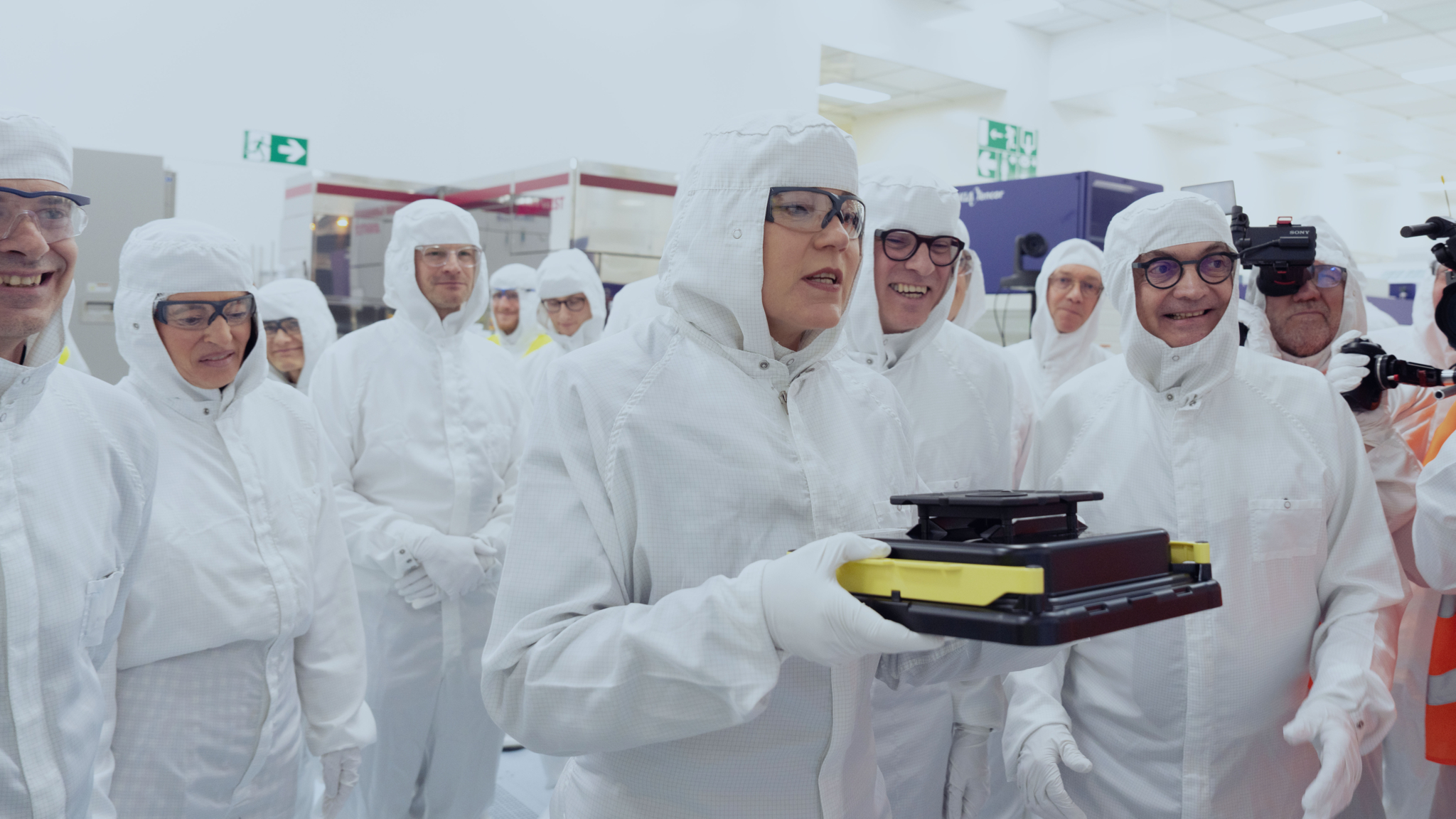
On February 9, 2026, the NanoIC pilot line was inaugurated by imec at its headquarters in Leuven. This is a landmark achievement for Europe’s semiconductor industry, turning the ambitions of the EU Chips Act into reality.
Backed by a €2.5 billion investment from the European Union, the Flemish government, and industry partners including ASML, the NanoIC pilot line will enable the development of beyond-2nm systems-on-chip, driving breakthroughs in AI, autonomous vehicles, personalized medicine, 6G networks, and quantum computing.
“Since announcing in May 2024 that imec would host the NanoIC pilot line, we’ve moved at full speed – accelerating tool acquisition and launching a comprehensive recruitment program. Today, that effort culminates in the inauguration of a 2,000m² cleanroom extension at the imec premises. It will house abest-in-class toolset, including ASML’s next-generation High NA EUV scanner that is scheduled to arrive mid-March,” said Luc Van den hove, CEO of imec.
The NanoIC pilot line will install more than hundreds of new tools, provided by the participants in NanoIC including imec, CEA-Leti (France), Fraunhofer (Germany), VTT (Finland), CSSNT-UPB (Romania) and Tyndall National Institute (Ireland).
In early February the pilot line released two Process Design Kits (PDKs) supported by Cadence and Synopsys. One is for the upcoming A14 process, and the other is for integrated DRAM, which is an important component for AI applications. By releasing the PDKs, NanoIC wants to enable researchers and smaller companies to explore the process’s workflows and design rules long before it is available.
Both PDKs, together with the previously launched N2 PDK, are available through Europractice. To encourage adoption and hands-on exploration, NanoIC will also host a dedicated workshop on the N2 and A14 PDK on March 25–26, 2026, and on the eDRAM PDK on May 26, 2026. These workshops will offer practical guidance, technical insights, and direct interaction with the development teams.
PDKs | NanoIC pilot line
Advanced PDK workshop: N2 and A14 nanosheet pathfinding and applications | imec
Advanced PDK Workshop: NanoIC’s IGZO‑based eDRAM PDK | imec
About the NanoIC Pilot line
Home | NanoIC pilot line
NanoIC is coordinated by the Belgian research institute Imec.
The pilot line will provide CMOS processes for nodes corresponding to 2 nm or less.
Source: Press release Imec inaugurates NanoIC pilot line | NanoIC pilot line